7 MOS Transistor
MOSFETs (metal-oxide-semiconductor field-effect transistors) (or MOS) are the pervasive switching semiconductor devices in digital integrated circuits (IC) and serve as transconductance components in analog ICs.This chapter focuses on analyzing and deriving the expressions of current in a long channel MOSFET.
7.1 Principle of Operation
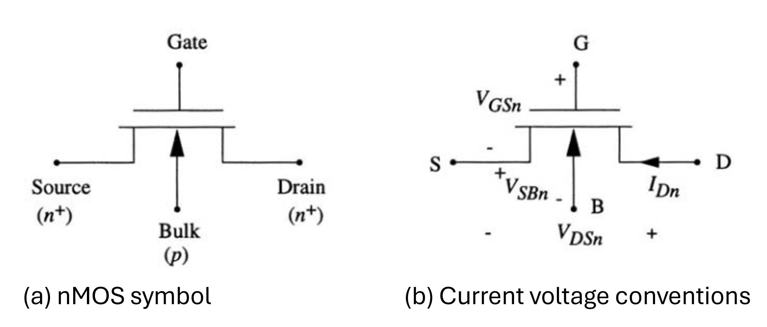
Figure 7.1(a) shows an n-channel MOSFET’s circuit symbol (n-FET or nMOS), a four-terminal device with gate, source, drain, and bulk terminals. Figure 7.1(b) depicts the device voltages. The gate acts as the control electrode and the gate source voltage (\(V_{GSn}\)) regulates the drain current (\(I_{Dn}\)) from the drain to the source. The drain current depends on \(V_{GSn}\) and the drain-source voltage (\(V_{DSn}\)), while the source-bulk voltage (\(V_{SBn}\)) has a minor influence.
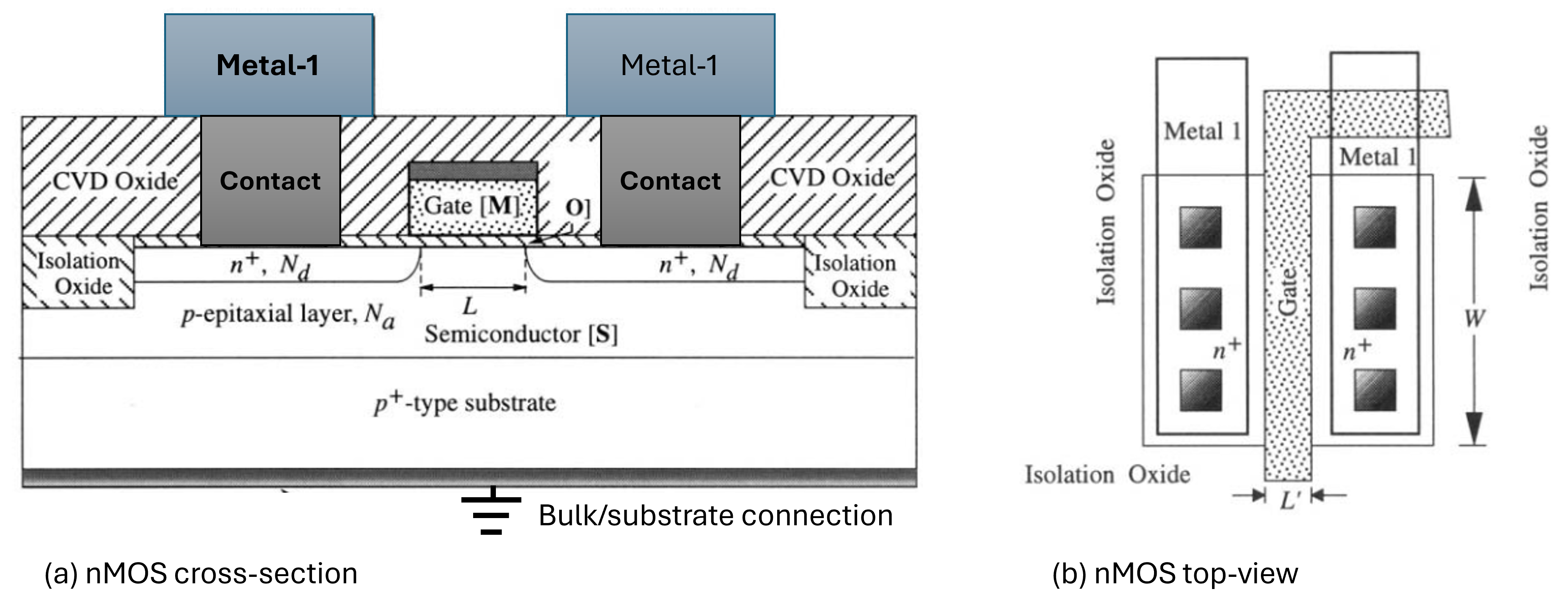
Figure 7.2 (a) shows an nMOS with a metal gate (M) on silicon dioxide (O) over p-type silicon (S). This structure forms a capacitor between the gate and the semiconductor. The drain and source terminals are on the sides, with a bulk electrode attached to the substrate. The length of the channel (\(L\)) between the drain and the source is crucial. Figure 7.2 (b)’s top view shows that the channel width (\(W\)) allows current flow, with the aspect ratio (W/L) important for design. The drawn channel length (\(L'\)) exceeds the electrical length (\(L\)).
The MOSFET current-voltage characteristics (\(I\)-\(V\)) rely on a threshold voltage (\(V_{Tn}\)) determined by the manufacturing parameters. CMOS technology usually uses enhancement-mode MOSFETs with a positive threshold voltage.
The MOS structure enables drain-to-source conduction due to its capacitor-like traits. A positive gate voltage induces negative charge in the semiconductor under the oxide via the field effect, altering surface charge distribution.
In an ideal n-channel MOSFET, when \(V_{GSn} < V_{Tn}\), it is in cutoff with zero current flow (\(I_d\)). Only immobile bulk charge exists under the gate, and the drain and source are separated by reverse-biased pn junctions.
When \(V_{GSn} \geq V_{Tn}\), an electron inversion layer is formed under the oxide, creating a conduction path from the drain to the source. Applying \(V_{DSn}\) generates an electric field in the channel, driving electrons from source to drain, resulting in a drain current (\(I_{Dn}\)).