5 Semiconductor IC devices
5.1 Introduction
The large-scale integration of electronic circuits is rooted in the invention and evolution of semiconductor devices. We will discuss electronic materials to explain the fundamental properties of semiconductors in IC design and their role in the success of integrated circuits.
| \(\mu -\Omega\) cm | \(m\Omega/\square\) | |
|---|---|---|
| Al | 2.65 | 26.5 |
| Cu | 1.68 | 16.8 |
| Au | 2.44 | 24.4 |
The fundamental materials in integrated circuits include metals, dielectrics, and semiconductors. Metals are used as conductors for interconnects because of their extremely low specific resistivity. Specific resistivity (\(\rho\)) is a property of the material that can be defined as resistance per unit volume expressed in SI units of \(\Omega m\) but more conveniently as \(\Omega cm\). The resistance of a rectangular piece of that material can be expressed as \(R=\rho\cdot l/A\), where \(l\) is the length and \(A\) is the cross-sectional area. In integrated circuit design, the height of the metal routing is fixed and is typically in the range of \(0.1\) to \(5\) micrometers (\(\mu m, 10^{-6} m)\) and the resistance is measured in unit squares as or \(\Omega/\square\). The specific resistance (in \(\Omega cm\)) and unit resistance (in \(\Omega/\square\)) of typical metals used in integrated circuits such as aluminum (Al), copper (Cu) and gold (Au) are tabulated in Table 5.1. Dielectric materials have extremely large specific resistances that provide electrical insulation for typical operating conditions. Specific resistances for semiconductors can vary enormously \(-\) from \(10^{-4} ~\Omega cm\) to \(10^{12} ~\Omega cm\).
The history of semiconductors began with Tomas Seebeck’s observation of lead sulfur (PbS) properties in 1821. Michael Faraday noted that semiconductor resistance decreases with rising temperatures, unlike conductors. Early applications include Werner von Siemens’ selenium photometer (1875) and Alexander Graham Bell’s wireless device (1878). The pivotal discovery of the Bipolar Junction Transistor (BJT) by Shockley, Bardeen, and Brattain in 1947 led to today’s integrated circuits with millions of devices in a single IC.
Electronic systems operate using a power supply formed by non-electric forces that separate charges to create a potential difference. Chemical forces generate batteries, while turbines produce AC, which is converted to DC voltages. This potential difference forms an electric field, driving current in the circuit. Manipulating this current with semiconductor devices in an integrated circuit is essential for intelligent systems like modern computers..
Semiconductor devices excel in integrated circuits due to their rapid conductivity changes, small size, and low energy use. They are manufactured at nanometer scales with switching speeds of 100 gigahertz, consuming nanowatts of power. Their conductivity can shift dramatically from insulator to conductor, representing digital zeros and ones. Understanding semiconductors like silicon involves studying the physics of their conductivity changes, which vary significantly with temperature as well.
Some excellent references for this subject matter are (Shur 1996), (Pierret 1996), (Streetman and Banerjee 2014), and (Gray and Searle 1969)
5.2 Energy Band Model
The energy band model explains the conduction properties of matter easily that we will introduce now using quantum mechanical properties of matter. Instead of explaining the model for a semiconductor crystal such as silicon, the basic principles can be explained using a much simpler atomic system, the isolated hydrogen atom. During the 1900s, the emission spectrum of heated gases did not agree with the contemporary physical model of continuous electron energy. In order to reconcile the discrepancy, in 1913 Neils Bohr proposed that the electrons can have only certain discrete allowed energy levels, called energy states.
For hydrogen atom the quantization of energy states is \(E_n = -E_B/n^2\) where \(n = 1,2,3,4,\ldots\) is called the energy quantum number and \(E_B\) is called the Bohr energy or the electron binding energy.
For hydrogen atom, Bohr energy \(E_B = 13.6 eV/n^2\)
Electron energies are expressed in electron volt (eV), the work done to move an electron across a potential difference of \(1~V\).
[\(1~eV = q\times 1V = 1.602\times 10^{-19} Joule\)]
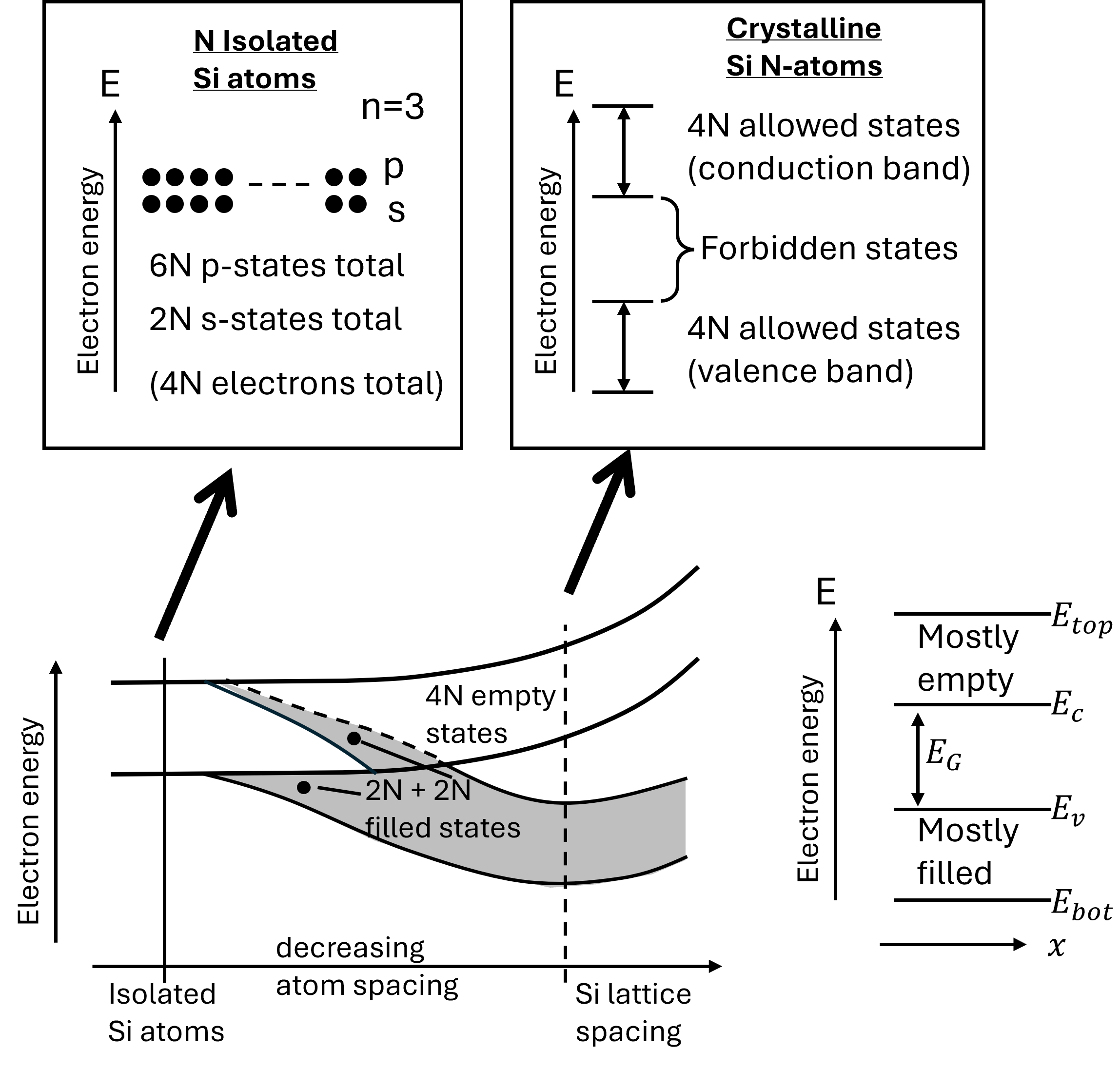
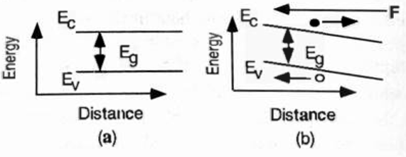
Let us now study the many electron energies of a Si crystal (Si), which is more complicated, but the basic principles still apply. The concept of band diagrams can be qualitatively conceived by starting with N-isolated Si atoms and observing the energy states as the atoms are brought closer and closer together (see Figure 5.1). Pauli exclusion principle plays an important role in determining energy states as the atoms are brought closer. The principle states that no more than two electrons can occupy each energy state. In a solid material, as many atoms (N) are brought closer, the energy states start to split to satisfy the exclusion principle. At the interatomic spacing of the lattice, the split energy levels form essentially continuous energy bands. However, these bands are separated by forbidden energy gaps that cannot be occupied by any electron. The magnitude of the forbidden energy gaps determines primarily the electrical properties of different materials. In filling the allowed energy states, electrons tend to gravitate to the lowest possible states. At room temperature in semiconductors and dielectrics, almost all of the states in the lower energy bands are filled by electrons, and the higher energy states are mostly empty. The upper band of the allowed states is called the conduction band; the lower band of the allowed states is called the valence band; and the gap between the two bands without any allowed energy states, the forbidden band or the energy band gap. An electron in the valence band needs energy equal to or greater than the energy band gap to transition from the valence band to the conduction band.
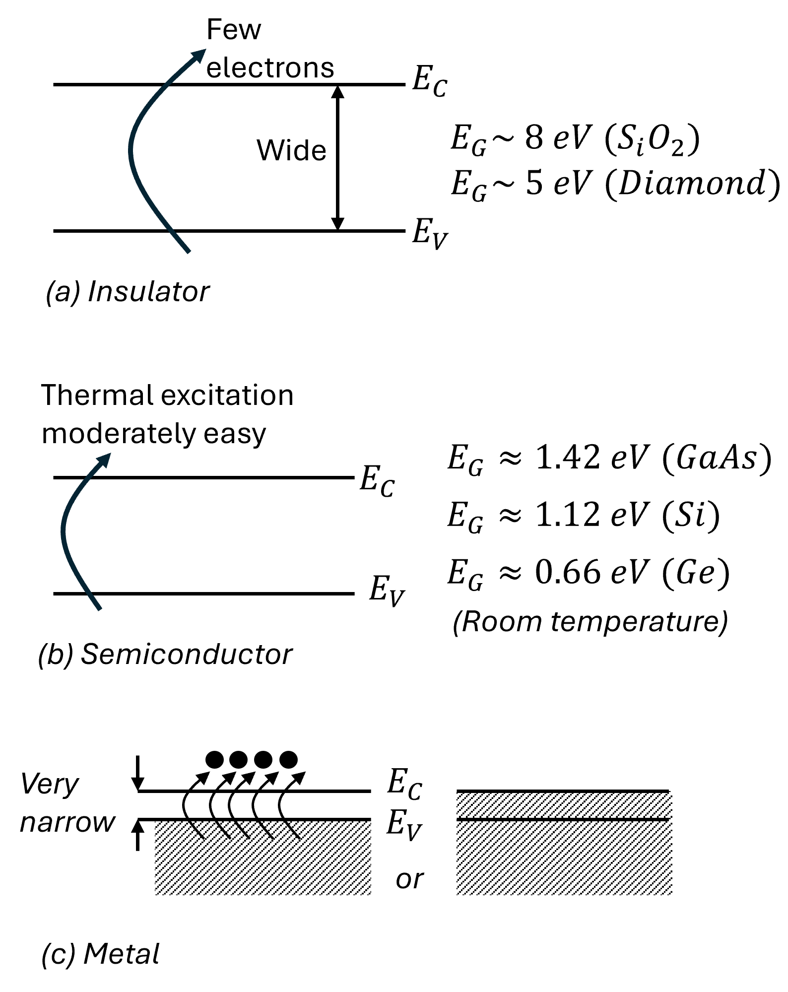
Typically, for semiconductors, the energy band gap, \(E_g\), varies between \(0.1~eV\) and \(3.5~eV\).
At room temperature (T=300K), \(E_G=1.42eV\) (GaAs), \(E_G=1.12eV\) (Si), and \(E_G=0.66eV\) (Ge).
In dielectric, the energy band gap is large and so the valence bands are completely filled and the conduction band is totally void of electrons making them perfect insulators. Typically for dielectrics, \(E_g\) is larger than \(5~eV\) (diamond) to \(8~eV~(SiO_2)\). In a metal, the lowest conduction band is partially filled with many electrons, making it an ideal conductor.
5.3 Carriers
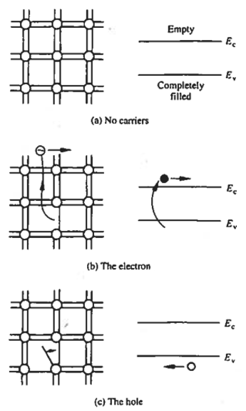
Carriers are the current-carrying entities within the semiconductor material and we are now in a position to introduce them, the semiconductor model having been well established. Referring to our bonding model, there are no carriers or possible current flow if no bonds are broken in the semiconductor solid. In the energy band model, this refers to a valence band which is completely filled with electrons and a conduction band which is completely devoid of electrons. This will be the case for a pure semiconductor like a silicon crystal at temperature \(T=0^\circ K\). Now, for an electron to carry current under the influence of an applied electric field, it has to break free from the bond, for example, the Si-Si bond. In terms of the energy band model, this refers to an electron from the valence band jumping over to the conduction band creating carriers; that is, electrons in the conduction band are carriers. Note that the energy required to break a bond is the same as the forbidden energy gap \(E_G\).
The average thermal energy of an electron, in equilibrium, is equal to \(3k_BT/2\) where, \(k_B\) is the Boltzmann constant and \(T\) is the temperature in degrees Kelvin. The generally accepted room temperature is \(27^\circ C\) or \(300~K\).
\(k_BT = 1.38\times 10^{-23} \frac{J}{K} \times 300~K = 0.026~eV\)
This energy is attributed to the electron’s thermal motion inside the crystal lattice that can be explained accurately using quantum mechanics. But an effective mass formulation is a simplified classical way of explaining the same phenomenon. This allows us to formulate the carriers as quasi-classical particles and employ classical particle relationships in most device analyzes. Using this formulation, the average thermal energy can be attributed to the average kinetic energy \(m^*_n v_{th}^2/2\) where \(m^*_n\) is the effective electron mass and \(v_{th}\) is called the electron thermal velocity.
The electron effective mass \(m^*_n\) is different from the free electron mass \(m^*_e\) which is \(9.11\times 10^{-31}kg\). For example, in silicon, \(m^*_n\approx 0.066~m_e\).
However, \(3k_BT/2\) is just the average energy, and the actual energies of an individual electron vary widely. A few electrons acquire enough thermal energy to jump into the conduction band.
Energy gap \(E_G\) of silicon (Si) is \(\approx 1.12 ~eV\) which is approximately 45 times larger than \(k_BT\) at room temperature!
Since there can be no current in the absence of an electric field, the random motions of the electrons compensate for each other. In the presence of an electric field, in addition to random motions, the electrons seem to drift in the direction of the electric with a so-called drift velocity which results in an electric current.
Now let us look at a phenomenon, unique to semiconductors, when an electron breaks free from a bond. It leaves a vacancy for another electron to break free from its bond and occupy this vacancy which in turn leaves another vacancy and so on leading to an appearance of a motion of a vacant electron of a positive charge \(q=-(-q)\) and an effective mass of \(m^*_p\). This motion is typically represented as a fictitious particle called a hole. This phenomenon can be imagined as analogous to the bubble in a fluid. In terms of the energy band model, jumping an electron to the conduction band creates a hole in an otherwise vast sea of filled states. This empty state, like a bubble in a fluid, moves about rather freely in the solid because of the cooperative motion of valence-band electrons that give room to this hole in motion. Like a free electron carrier, when an electric field is applied to this semiconductor, the hole, an apparent positive electron, will move in the direction of the electric field, giving rise to electric current.
5.4 Band Diagrams
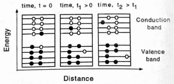
Band diagrams are a very efficient way of illustrating electrical properties of semiconductor materials and devices without going into the detail atomic or molecular structure of the material. As shown in Figure 5.4, the band diagram represents the electrical energies allowed within the semiconductor as a function of position, where the increase in energy \(E\) upward represents the total energy of electrons. The charge carriers or free charge carriers start to occupy the lowest energy states in the conduction band which are lower edge of the conduction band (\(E_C\)) and upper edge of the valence band (\(E_V\)) for electrons and holes, respectively.
Therefore, to analyze or understand the electrical behavior of a uniform semiconductor material it is typically sufficient to study the material properties with the band edges only. Normal operation is assumed here without any external disturbances, where the electric field, magnetic field, temperature gradient, and stress-induced effects are negligible.
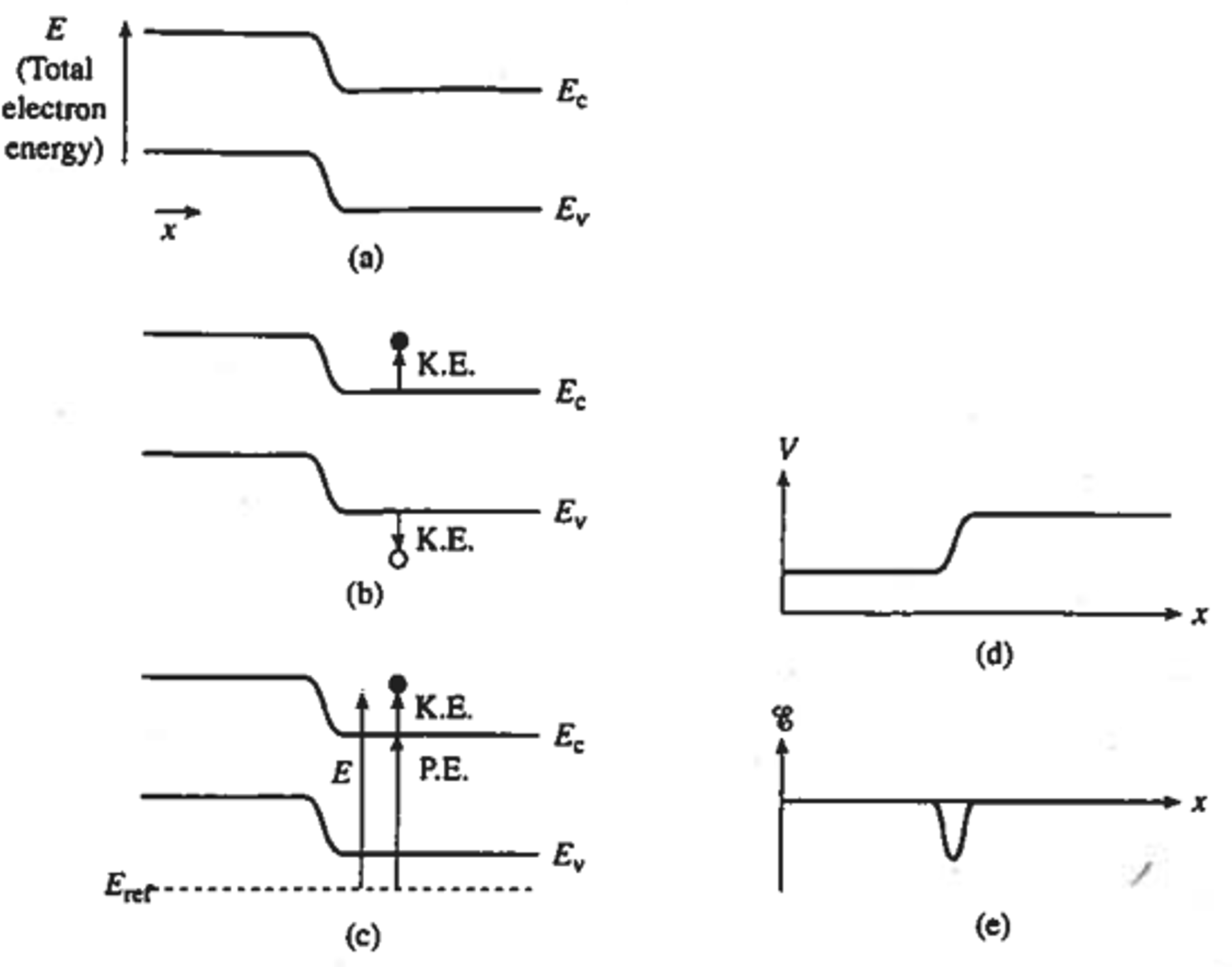
On careful examination of the band diagram, we can show that an energy equal to the bandgap, \(E_G = E_C-E_V\), is required to break an atomic bond to create motionless electrons and holes occupying \(E_C\) and \(E_V\), respectively. Therefore, we can interpret the edges of the band \(E_C\) and \(E_V\) as the potential energy of the electron and hole, respectively, with reference to an arbitrary energy level \(E_{ref}\).
Potential Energy: \(P.E.=E_C-E_{ref}\) NOTE: Show PE and KE on the diagram itself.
Any energy in excess of \(E_G\) will result in the kinetic energy shown in figure Figure 5.5, with the carriers moving rapidly in the lattice. The potential energy is the key to relating the positional variations in the energy band with the electric field within the semiconductor. The potential energy (\(P.E.\)) of an electron (\(-q\)) can be expressed as \(-qV\), where \(V\) is the electrostatic potential at a given point with reference to an arbitrary constant. The potential can be expressed in terms of \(E_C\) using the relationship shown previously between \(P.E.\) and \(E_C\).
\[ P.E. = -qV = E_C - E_{ref} \]
\[ V=-1/q(E_C - E_{ref}) \]
The band diagram of a piece of semiconductor with the presence of an electric field \(E\) is shown as an example in Figure 5.6 (b). The bands are tilted with a slope of \(-qE\) popularly known as band bending. Since electrons are negatively charged, the direction of the forces on electrons is opposite to that of the electric field. The forces on the holes are in the same direction as the electric field. Consequently, the electrons and holes move in opposite directions.
\[ E=-\nabla V \text{ or,} \]
\[ E_x = -dV/dx \]
\[ E_x = \frac{1}{q}\frac{dE_C}{dx} \text{ or,} \]
\[ E_x = \frac{1}{q}\frac{dE_V}{dx} \text{ or,} \]
\[ E_x = \frac{1}{q}\frac{dE_i}{dx} \]
Using basic electrostatic laws, the relationship between the potential \(V\) and electric field \(\vec{E}\) can be established. For quick analysis by inspection, the \(V\) and \(x\) relationship can be found simply by “inverting” \(E_C\) (or \(E_V\)) and to determine the \(\vec{E}\) versus \(x\) relationship, simply note the slope of \(E_C\) (or \(E_V\)).
A pure semiconductor that contains an insignificant amount of impurity atoms is commonly referred to as an intra-intrinsic semiconductor. In other words, it is a semiconductor whose properties are native to the material without any external additives. In an intrinsic semiconductor, the electron concentration in the conduction band and the holes in the valence band are negligible compared to the number of available energy states within \(k_B T\) from the edges of the band.
| Material | \(n_i\) |
|---|---|
| Si | \(1\times 10^{10}/cm^3\) |
| Ge | \(2\times 10^{13}/cm^3\) |
| GaAs | \(2\times 10^{6}/cm^3\) |
In general, the number of electrons and holes per cubic-centimeter are defined as \(n\) and \(p\) respectively. Since electrons and holes are created in pairs in an intrinsic semiconductor, the concentrations of electrons and holes are the same and are represented as \(n_i\) where \(n_i=n=p\). The intrinsic electron-hole concentrations in some popular semiconductor material are tabulated in Table 5.2. Although the absolute concentration appears to be a large number, it is an insignificant number compared to the density of atoms in the material. For example, in silicon (Si) there are \(5\times 10^{22}~atoms/cm^3\). An intrinsic concentration of \(n_i\approx 10^{10}/cm^3\) is less than one broken bond in \(10^{13}\) atoms.
| Donors (V) | Acceptors (III) |
|---|---|
| \(P^*\) | \(B^*\) |
| \(As^*\) | \(Ga\) |
| \(Sb\) | \(In\) |
| \(Al\) |
5.5 Doping
Doping is a semiconductor engineering method to change the electron or hole concentration of the native material by many orders of magnitude. As a result, the conductance of the semiconductor varies by a large magnitude. Doping is a routine method in IC fabrication in which semiconductor impurity atoms called dopants are added to the pure semiconductor material. Dopants that increase the electron concentration of the native semiconductor material are called donors. Consequently, acceptors are dopants that increase hole concentration.
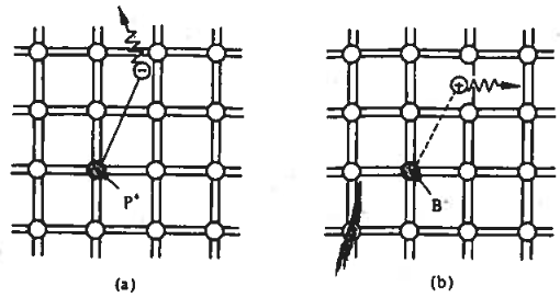
Commonly used silicon dopants are listed in Table 5.3. Phosphorous dopants, closely followed by arsenic, are the most commonly used donor dopants to increase the electron concentration. Boron is the most commonly used acceptor dopant for increasing hole concentration.
The donors are all from the Column-V of the Periodic Table of Elements and correspondingly, the acceptors are from Column-III.
As shown in Figure 5.7, using the bonding model, when a Column-V element replaces a silicon atom, four valence electrons bond with nearby silicon atoms, while the fifth is weakly bound to the donor site. At room temperature, this electron gains enough energy to become a conduction band carrier without increasing hole concentration, leaving an immobile ion.
The binding energy of a Phosphorous donor electron in silicon is about \(0.045~eV\) compared to \(1~eV\) for Si-Si atom.
A semiconductor doped with donors is called an n-type semiconductor.
\(n+\) and \(n-\) refers to heavily and lightly doped n-type semiconductor.
At room temperature or above, each donor atom in an n-type semiconductor contributes one electron to the conduction band, making the electron concentration in the conduction band approximately equal to the donor concentration, typically expressed in \(atoms/cm^3\).
A Column-III acceptor element replaces a silicon atom, accepting an electron from a neighboring Si-Si bond to complete its bonding. This creates a hole that can move through the lattice, depicted as a hole weakly bound to the acceptor site.
The binding energy of a Boron acceptor hole in silicon is about \(0.045~eV\).
A semiconductor doped with an acceptor is called an p-type semiconductor. At room temperature or hotter temperatures, each acceptor atom in an p-type semiconductor supplies one hole to the valence band and therefore the hole concentration, \(p\), in the valence band is approximately equal to the acceptor concentration, \(N_A\), typically expressed in \(atoms/cm^3\).
\(p+\) and \(p-\) refer to heavily and lightly doped n-type semiconductor, respectively.
An important relation used in the analysis of semiconductor devices is the constant product of hole and electron concentration, \(p\) and \(n\), for a given temperature, which can be conveniently written as
\[ np = n_i^2 \]
where, \(n_i\) is the electron or hole concentration in an intrinsic semiconductor material at that temperature.
Integrated circuits for commercial, industrial, or military use must perform across a wide temperature range, \(-40^\circ~C\) to \(125^\circ~C\). Understanding carrier concentration’s temperature dependence is crucial for semiconductors.
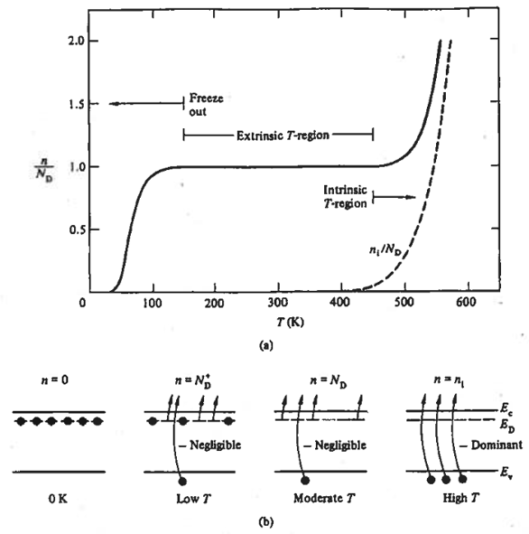
Figure 5.8 illustrates a carrier concentration vs. temperature plot for Si doped with phosphorus \(N_D = 10^{15}/cm^3\), highlighting the dependence of carrier concentration on temperature. The majority carrier concentration \(n\) remains near the donor concentration \(N_D\) from \(-125^\circ~C\) to \(175^\circ~C\) (\(\approx~150~K\text{ to } 450~K\)), known as the extrinsic temperature range, which is typical for integrated circuits’ operating temperatures.
The carrier concentration varies with temperature. Below the extrinsic range, donor electrons lack energy to enter the conduction band. Around temperature \(150~K\), most donor electrons are in the conduction band. As temperature rises, electrons from Si-Si bonds are excited but remain below \(N_D\). Beyond the extrinsic range, Si-Si bond electrons surpass donor electrons, equating carrier concentration to an intrinsic semiconductor in the intrinsic range.
5.6 Electric Current
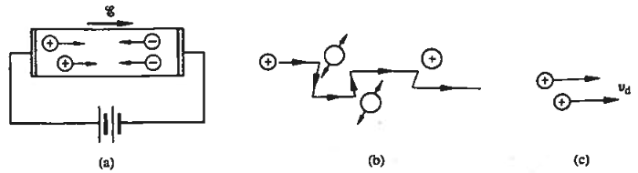
The electric current through a uniform semiconductor can now be studied in it’s simplest form using basic electrostatic laws. When a weak electric field is applied across a semiconductor material, a so-called drift velocity is superimposed on top of the chaotic thermal motion of electrons in the conduction band and holes in the valence band.
The drift velocities, \(v_n\) and \(v_p\), of the electrons and holes are proportional to the electric field, \(\vec{E}\)
\[ v_n = -\mu_n\vec{E} \]
\[ v_p = \mu_p\vec{E} \]
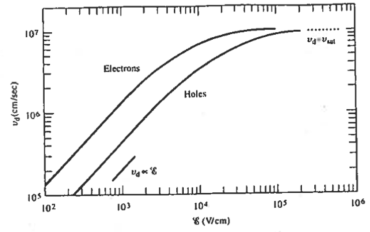
where, \(\mu_n\) and \(\mu_p\) are called the electron mobility and the hole mobility, respectively. Note that \(v_p\) and \(v_n\) are proportional to \(\vec{E}\) for weak electric fields. At strong electric fields \(v_p\) and \(v_n\) become independent of \(\vec{E}\) (See Figure 5.11).
Notice that the direction of the current: \(v_p\) coincides with the direction of the electric field and \(v_n\) is opposite to the direction of the electric field because of the carriers charged opposite.
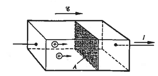
The flow of electric current in a uniform semiconductor material can be determined by evaluating the number of charge carriers passing through a unit cross-section each second. For the p-type semiconductor bar with a unit cross-sectional area depicted in Figure 5.11, the hole current density, \(J_P\), can be straightforwardly defined as:
\[ J_P = qp v_p \]
In order to relate the current to the applied electric field, one can substitute the hole drift velocity \(v_p\) with the formula \(\mu_p\vec{E}\).
\[ J_P = qp\mu_p\vec{E} \]
In a similar way, the current density for electrons can be represented as
\[ J_N = qn\mu_n\vec{E} \tag{5.1}\]
Observe that the electrons move in the opposite direction to the applied electric field (\(v_n = -\mu_n\vec{E}\)). However, the current density flows in the opposite direction of this drift velocity due to the negative charge of the electrons (\(J_N = -qn v_n\)). Consequently, as stated in Equation 5.1, the resulting electron current aligns with the direction of the applied electric field.
In semiconductors where both electrons and holes function as charge carriers, the overall current density is represented by
\[ J = q\vec{E}\left({n\mu_n + p\mu_p}\right) \tag{5.2}\]
In n-type materials, the contribution from hole-current can often be overlooked since the hole concentration, \(p\), is significantly smaller in comparison to the electron concentration, \(n\). Similarly, in p-type semiconductors, the electron current can be disregarded.
Equation 5.2 is commonly referred to as Ohm’s Law and can be expressed in its well-known format.
\[ I = \frac{V}{R} \tag{5.3}\]
where \(I=J \cdot A\) represents the overall current passing through a cross-sectional area \(A\) of the sample. With the electric field magnitude \(E\) being constant, the voltage differential over the semiconductor length \(L\) is given by \(V = E \cdot L\), and the resistance of the sample can be written as
\[ R=\frac{L}{\sigma \cdot A} \tag{5.4}\]
where \(\sigma=q\left({n\mu_n + p\mu_p}\right)\) (see Equation 5.2). Keep in mind that Ohm’s law generally applies to weak electric fields, a condition seldom met in contemporary integrated circuits with feature sizes below a micrometer. Nonetheless, it remains a valuable expression for grasping the basic principles of current transport in semiconductors.
5.7 Diffusion
The second mechanism influencing the overall current in a semiconductor is diffusion. This process involves the distribution of particles due to random thermal motion, moving from areas of higher particle concentration to areas of lower particle concentration, ultimately achieving an even distribution. This can be likened to a drop of ink dispersing in a glass of water, where the ink gradually spreads out uniformly across the water.
In a general three-dimensional case the concentration profiles will be expressed as gradients:
\[ J_{P|diff} = -qD_P\nabla p \tag{5.5}\]
\[ J_{N|diff} = qD_N\nabla n \tag{5.6}\]
In a one-dimensional scenario, the overall current can now be described as
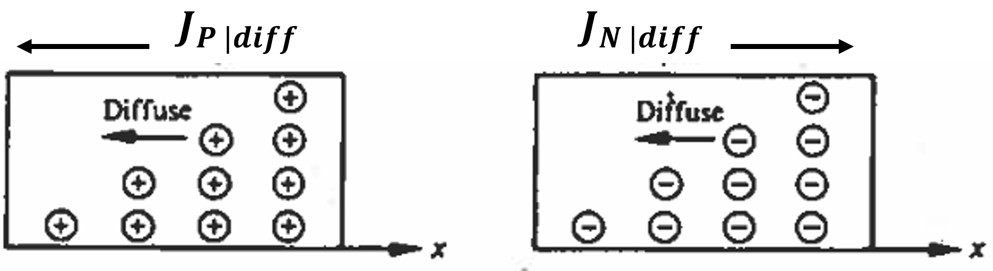
\[ J = \underbrace{q\vec{E}\left({n\mu_n + p\mu_p}\right)}_{drift} + \underbrace{q\left({D_N\frac{dn}{dx} - D_P\frac{dp}{dx}}\right)}_{diffusion} \]
where \(D_N\) and \(D_P\) are the diffusion constants for electrons and holes respectively. For a positive concentration gradient (\(dp/dx > 0\) and \(dn/dx > 0\)), as shown in Figure 5.12, both holes and electrons will diffuse in the negative-x direction. Therefore, \(J_{P|diff}\) will be in the negative x direction and \(J_{N|diff}\) in the positive x direction.
Both drift and diffusion arise from the random thermal movement of carriers. As a result, the mobility \(\mu\) and the diffusion coefficient \(D\) are interconnected through the Einstein relationship:
\[ D_N/\mu_n = D_P/\mu_p = kT/q \tag{5.7}\]
With a foundational understanding of semiconductor materials, we can now delve into the electronics of semiconductor devices within integrated circuits, beginning with p-n junctions and progressing to the pivotal component in integrated circuits, the MOSFET.
5.8 pn Junctions
Junctions are fundamental to understanding any semiconductor device since these junctions are formed when two different materials come into contact or the same semiconductor material with different doping.
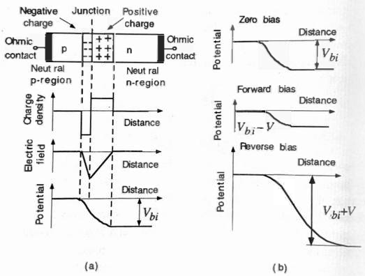
p-n junctions occur where an \(n\)-type semiconductor meets a \(p\)-type semiconductor. In equilibrium, holes migrate from the \(p\) region to the \(n\) region, moving from an area of higher concentration to one of lower concentration. This movement leaves behind a zone of immobile, negatively charged acceptor ions near the junction. Similarly, electrons move from the \(n\) region to the \(p\) region, resulting in an accumulation of positively charged donor ions near the junction (see Figure 5.13). The interface thus forms a space charge region or depletion region, characterized by the absence of holes in the \(p\)-region and electrons in the \(n\)-region. These immobile charges on either side generate a potential barrier known as the contact potential \(V_0\), also referred to as a built-in potential, which ultimately inhibits further crossing of electrons and holes across the interface.
In the n-region, the majority of electrons reside in energy states near the conduction band edge \(E_C\), having minimal thermal energy. As energy levels rise from the band edge, the quantity of electrons diminishes exponentially, leaving only a small number able to surpass the built-in potential barrier. Upon crossing, the built-in electric field moves them to the p-side. Likewise, on the p-side, a similar process occurs with holes, maintaining a net current of zero.
Under equilibrium conditions, the overall current resulting from both drift and diffusion processes, such as for holes, sums to zero.
\[ \frac{J_{P_x}}{q} = \mu_{p_x} E_x - D_p \frac{d p_x}{dx} = 0 \tag{5.8}\]
By applying this condition, the relationship between the contact potential and the doping concentrations on each side of the junction can be determined as:
\[ V_0 = \frac{kT}{q}\ln{\frac{N_A N_D}{n_i^2}} \tag{5.9}\]
assuming the doping concentration dominates on both sides. Then, applying the equilibrium condition \(p_pn_p = n_i^2 = n_nn_p\), the #eq-semi-dev-contact-v can be reformulated into a more advantageous form as:
\[ \frac{p_p}{p_n} = \frac{n_n}{n_p} = e^{qV_0/kT} \tag{5.10}\]
where \(p_p\) and \(p_n\) signify the hole densities on the \(p\) and \(n\) regions, respectively, while \(n_n\) and \(n_p\) indicate the electron densities on the \(n\) and \(p\) regions, respectively.
Evaluate the situation of forward bias, where a voltage \(V_F\) is applied across the p-side relative to the n-side. This causes a linear reduction in the potential barrier by \(V_F\). However, the count of electrons at the junction capable of overcoming the barrier grows exponentially with \(V_F\). As electrons constitute minority carriers in the \(p\) region, the carrier concentration near the contact reduces due to a recombination process, resulting in forward current driven by diffusion.
Therefore, the forward current \(I\) is anticipated to be an exponentially increasing function relative to the applied forward voltage \(V_F\). The overall relationship between \(I\) and \(V\) can be represented in its general expression.
\[ I = I_S(e^{qV_F/kT} - 1 ) \tag{5.11}\]
Equation 5.11 represents the ideal diode equation, which forecasts that the minor reverse-bias current will settle at \(-I_S\). This saturation persists even at low reverse bias voltages exceeding several \(kT/q\). The current arises from a limited number of bias-independent minority carriers being driven by the electric field upon entering the depletion region.
See (Pierret 1996) (p-239) for a treatment on Recombination-Generation (RG) process. Minor concentration at the edge of the depletion can be derived using the linear profile and the current equation can be derived from it (Pierret 1996) (p-245) (Gray and Searle 1969) (p-134)
5.9 pn Junction Current
To enhance our comprehension of the current flow through the pn junction, we can now incorporate some quantitative analysis. Staying true to the approach of this text, the quantitative explanation will be kept quite brief, primarily by presenting key principles as given assumptions or as a priori knowledge sourced from references.
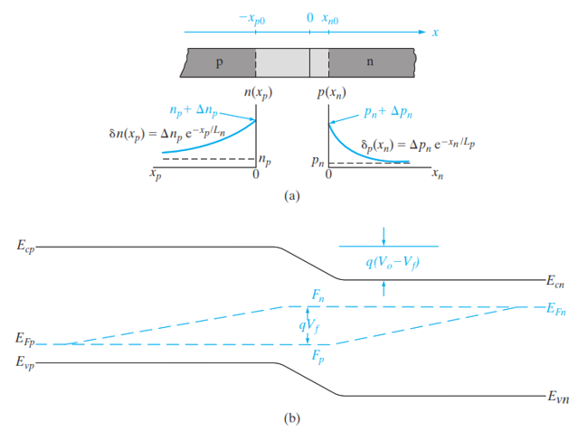
The present derivation can be arranged by considering three separate electrostatic regions of a pn junction as illustrated in Figure 5.14. These regions include: the quasi-neutral p-region characterized by a zero electric field, the space charge region with a nonzero electric field, and the quasineutral n-region also with a zero electric field. Previous studies have elaborated extensively that the ideal forward bias current can be determined by examining the current within the quasi-neutral region, attributable to the low-level injection of minority carriers at the boundaries of the depletion region, \(x_{p0}\) and \(x_{n0}\). Under forward bias \(V_F\), the equilibrium ratio of hole concentrations (Equation 5.10) transforms into:
\[ p(x_{p0}) = p(x_{n0}) e^{q(V_0-V_F)/kT} \tag{5.12}\]
In low-level injection scenarios, the alteration in the majority carrier concentration is generally negligible (\(p(x_{p0}) = p_p\)). By substituting Equation 5.10 into Equation 5.12, the concentration of minority holes at \(x_{n0}\) can be represented as follows:
\[ p(x_{n0}) = p_n e^{qV_F/kT} \tag{5.13}\]
Take into consideration that Equation 5.13 is originally formulated for a forward-biased junction, but it remains applicable for reverse bias by altering the sign of the voltage to negative. Under this condition, the carrier concentration falls below the equilibrium level. The concentration of excess minority carriers on both the p-side and n-side is given by:
\[ \Delta p_n = p(x_{n0}) - p_n = p_n \left({e^{qV_F/kT} - 1}\right) \]
\[ \Delta n_p = n(x_{p0}) - n_p = n_p\left({e^{qV_F/kT} - 1}\right) \tag{5.14}\]
The diffusion theory suggests that minority carriers are injected at the boundaries of the space charge region, resulting in a stable concentration of \(\Delta p_n\) holes in the \(n\)-type material at \(x_{n0}\) and \(\Delta n_p\) electrons in the \(p\)-type material at \(x_{p0}\). This injection initiates a distribution of minority carriers, which follows the diffusion equation.
\[ \delta p(x_p) = \Delta p e^{-x_p/L_p} \]
\[ \delta n(x_n) = \Delta n e^{-x_n/L_n} \tag{5.15}\]
where \(L_p\) and \(L_n\) represent the diffusion lengths for holes and electrons, respectively. It is also presumed that the dimensions of the \(p\) and \(n\) materials exceed their corresponding diffusion lengths. By incorporating Equation 5.14 into the diffusion equation, the distribution of minority carriers can be represented as follows:
\[ \delta p(x_p) = p_n\left({e^{qV_F/kT} - 1}\right) e^{-x_p/L_p} \]
\[ \delta n(x_n) = n_p\left({e^{qV_F/kT} - 1}\right) e^{-x_n/L_n} \tag{5.16}\]
In the \(n\) material, the diffusion current of holes, and in the \(p\) material, the diffusion current of electrons can be determined by utilizing the diffusion component of the total current as described in Equation 5.8 :
\[ J_p(x_n) = -qD_p\frac{d\delta p(x_n)}{dx_n} = q \frac{D_p}{L_p}\delta p(x_n) \]
\[ J_n(x_p) = qD_n\frac{d\delta n(x_p)}{dx_p} = q \frac{D_n}{L_n}\delta n(x_p) \tag{5.17}\]
The total current can be now calculated by adding the hole and electron current evaluated at \(x_{n0}\) and \(x_{p0}\) respectively:
\[ I = qA\left({\frac{D_p}{L_p}p_n + \frac{D_n}{L_n}n_p}\right) \left({e^{V_F/kT} -1}\right) \]
or,
\[ I = I_S \left({e^{V_F/kT} -1}\right) \tag{5.18}\]
where, \(A\) is the area of the \(pn\) junction. Equation 5.18 is the diode equation, that has the same form as the qualitative expression in Equation 5.11 .
To determine the reverse bias current, substitute the forward bias voltage \(V_F\) with the negative value of the reverse bias voltage \(-V_R\). When \(V_R\) exceeds a few times \(kT/q\), the complete current becomes equivalent to the reverse saturation current:
\[ I = -qA\left({\frac{D_p}{L_p}p_n + \frac{D_n}{L_n}n_p}\right) = -I_S \tag{5.19}\]