3 Linear Circuits
3.1 Introduction
This chapter introduces linear circuits, essential to many electronic systems. We define linearity, focusing on homogeneity (proportionality) and additivity (superposition), which are key for analysis. We explore the voltage-current relationships in resistors, capacitors, and inductors using idealized models, and examine ideal voltage and current sources. We’ll focus on Kirchhoff’s Current Law (KCL) and Kirchhoff’s Voltage Law (KVL), foundational for circuit analysis. Nodal and mesh analysis, based on KCL and KVL, allow for solving voltages and currents in complex circuits. The superposition principle offers a method for analyzing multiple sources. Mastery of these concepts enables analysis of various linear circuits.
3.2 What are Linear Circuits ?
All the analysis techniques we will cover in this text are for linear circuits. Therefore, it’s beneficial to understand the definition of linear circuits. Briefly, a linear circuit adheres to the principles of linearity, namely homogeneity and additivity. Mathematically, these properties can be expressed as follows.
\[ f(Kx) = Kf(x) \text{ (homogeneity)}\]
where \(K\) is a scalar constant with the homogeneity property also known as proportionality, and
\[ f(x_1+x_2) = f(x_1) + f(x_2) \text{ (additivity)}\]
where the additive property is also known as superposition
The superposition and proportionality principle is also employed to assess the linearity of a circuit. For instance, in the case of a two-terminal circuit whose linearity is uncertain, we can utilize linearity principles to ascertain this property.
3.3 Basic Circuit Analysis
PASSIVE DEVICE (R,L,C) \(I-V\) characteristics has been derived. Although these devices are often non-linear in practice, we will use their linear models, known as circuit elements, and apply the following linear equations:
\[Resistor: v = iR\]
also known as Ohm’s law,
\[Capacitor: i = C\frac{dv}{dt}\]
\[Inductor: v = L \frac{di}{dt}\]
Using the principles of linearity, prove that the linear models of the passive RLC elements are linear.
The capacitor and inductor are non-dissipative devices but resistor is not, and the power dissipated by it is given by
\[ p = v^2/R\]
or,
\[ p = i^2 R\]
Determine the current flowing through a \(3.3 k\Omega\) resistor when \(3.3 V\) is applied across it, and calculate the power it dissipates.
A resistor remains linear when voltage and current are within its power rating limits. For a \(10~k\Omega\) resistor with a power rating of \(0.25 W\), determine the maximum current and voltage to keep it within its linear range
IDEAL SOURCES are essential for electronic circuits to function and are represented by two elements: voltage sources and current sources.
The \(i–v\) characteristic of an ideal voltage source is described by the following element equations:
\[ v=v_s \text{ and } i=\text{any value}\]
where, \(v_s\) is voltage across the source and \(i\) is the current flowing through it.
The \(i–v\) characteristic of an ideal current source is described by the following element equations:
\[ i=i_s \text{ and } v=\text{any value}\]
where, \(s_s\) is the current flowing through the source and \(v\) is the voltage across it.
In circuit analysis, the voltage or current from ideal sources is called a forcing or driving function, as it triggers a circuit response. Time-varying voltage or current is typically denoted as \(v(t)\) or \(i(t)\).
CONNECTION CONSTRAINTS are activated when devices are connected within a circuit. Two essential principles governed by connection constraints are Kirchhoff’s current law (KCL) and Kirchhoff’s voltage law (KVL).
3.3.1 Kirchhoff‘s Current Law (KCL)
Kirchhoff’s first law is founded on the conservation of charge principle. Kirchhoff’s current law (KCL) asserts that
the algebraic sum of the currents entering a node is zero at every instant.
When summing currents algebraically, consider each device’s reference direction: assign a positive sign if directed into the node, and a negative sign if directed away.
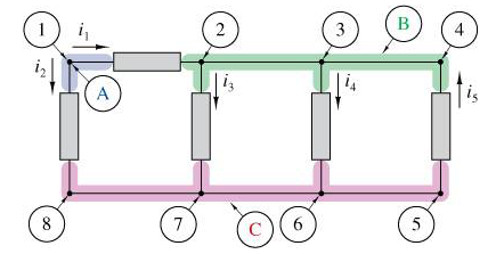
Applying this convention to the nodes in Figure 3.1, we obtain the following set of KCL connection equations:
\[\text{Node A: } -i_1 - i_2 = 0\] \[\text{Node B: } i_1 - i_3 - i_4 + i_5= 0\] \[\text{Node C: } i_2 + i_3 + i_4 - i_5= 0\]
The KCL equation at node A indicates that the reference direction for currents \(i_1\) and \(i_2\) is away from node A, not that they are negative. Similarly, the equation at node B could be expressed as
\[ i_1 + i_5 = i_3 + i_4 \]
This example demonstrates a different formulation of KCL:
The sum of the currents entering a node equals the sum of the currents leaving the node.
Another general principle that can be easily derived from KCL:
In a circuit containing a total of N nodes, there are only \(N – 1\) independent KCL connection equations.
The current equations specified at \(N – 1\) nodes encapsulate all the independent connection constraints derivable from the Kirchhoff’s Current Law (KCL).
Note that the three parallel elements in Figure 3.1 can be replaced by one equivalent element, which can generally be stated as:
Two circuits are said to be equivalent if they have identical \(i–v\) characteristics at a specified pair of terminals.
For example, if the 3 elements were resistors \(R_1, R_2, R_3\), they can be replaced with an equivalent resistor of value \(R_1R_2R_3/(R_1+R_2+R_3)\).
3.3.2 Kirchhoff’s Voltage Law (KVL)
Kirchhoff’s second circuit law is rooted in the energy conservation principle. According to the Kirchhoff voltage law (KVL),
the algebraic sum of all voltages around a loop is zero at every instant.
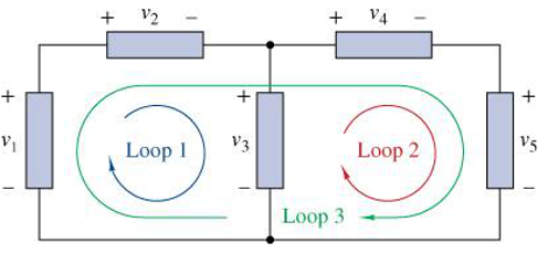
Three loops in Figure 3.2 show the circuit. A voltage receives a positive sign when moving from “+” to “–” and a negative sign from “–” to “+.” The loop’s clockwise traversal gives these KVL equations.
\[ \text{Loop 1: } -v_1 + v_2 + v_3 = 0 \] \[ \text{Loop 2: } -v_3 + v_4 + v_5 = 0 \] \[ \text{Loop 3: } -v_1 + v_2 + v_4 + v_5 = 0 \]
Two signs are linked to each voltage. The first sign is used when formulating the KVL connection equation. The second sign depends on the real polarity of the voltage compared to its designated reference polarity.
A general principle can be derived from KVL :
For a circuit that includes \(E\) number of two-terminal elements and has \(N\) nodes, only \(E - N + 1\) independent Kirchhoff’s Voltage Law (KVL) equations can be formed.
When voltage polarities or current directions are missing in a circuit diagram, they need to be set arbitrarily before analysis. These assignments don’t reflect the actual circuit conditions. If the assumed direction and polarities match the actual ones, the response’s sign will be positive; otherwise, it will be negative.
In other words, the sign of the answer together with the assigned polarities and directions tells us the actual voltage polarity or current direction.
In the passive sign convention, we can choose either the + voltage reference or the current reference arrow for a two-terminal element, but not both simultaneously. Once the voltage reference is set, the current arrow must enter the terminal with the + mark. Conversely, if the current reference is chosen first, the + voltage reference is applied to the same terminal.
3.4 Circuit Analysis Techniques
We can apply Ohm’s and Kirchhoff’s laws to develop two key circuit analysis techniques: nodal analysis, using Kirchhoff’s current law (KCL) and mesh analysis, using Kirchhoff’s voltage law (KVL). These techniques are crucial to any circuit analysis. By developing these methods, we can analyze almost any circuit by forming and solving simultaneous equations to find currents or voltages. One solution for these equations is Cramer’s rule, which calculates circuit variables using determinant quotients.
3.4.1 Nodal Analysis
Nodal analysis, or node-voltage analysis, analyzes circuits by using node voltages as variables, simplifying the process and reducing the number of simultaneous equations. It focuses on determining node voltages and follows three steps for a circuit with n nodes without voltage sources.
Select a reference node. Assign a voltage \(v_1, v_2, \ldots , v_{n-1}\) to the remaining \(N– 1\) nodes.
Apply KCL to each of the \(N-1\) non-reference nodes. Use Ohm’s law to express the branch currents in terms of node voltages.
Solve the resulting simultaneous equations to obtain the unknown node voltages.
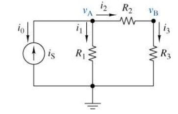
The circuit in Figure 3.3 illustrates node-voltage equation formulation, identifying a reference node (ground), four currents (\(i_0\), \(i_1\), \(i_2\), \(i_3\)), and two node voltages (\(v_A\), \(v_A\)).
At the two nodes that are not used as references, the KCL constraints can be stated as follows:
\[ \text{Node A: } -i_0-i_1-i_2 = 0\] \[ \text{Node B: } i_2-i_3 = 0\]
By applying the core principles of node analysis, we can connect element currents with node voltages through the corresponding element equations.
\[\text{Resistor} R_1\text{: } i_1 = \frac{v_A}{R_1} \] \[\text{Resistor} R_2\text{: } i_2 = \frac{v_A-v_B}{R_2} \] \[\text{Resistor} R_3\text{: } i_3 = \frac{v_B}{R_3} \] \[\text{Current source: } i_0 = -i_S \]
We formulate six equations for six unknowns, four currents of the element, and two node voltages. The right side of these equations involves unknown node voltages and the input signal \(i_S\). By substituting device constraints into the KCL equation and rearranging terms, we derive the following standard form:
\[ \text{Node A: } \left({\frac{1}{R_1}+\frac{1}{R_2}}\right) v_A - \frac{v_B}{R_2} = i_S\] \[ \text{Node B: } \frac{v_A}{R_2} + \left({\frac{1}{R_2}+\frac{1}{R_3}}\right) v_B = 0\]
In this standard form, unknown node voltages are on one side, and independent sources on the other, easing analysis. By eliminating element currents, the circuit is reduced to two linear equations with two unknown node voltages.
The node-voltage method simplifies solving to \(N– 1\) equations. With \(E\) elements, the reduction from \(2E\) to \(N– 1\) is notable in circuits having many elements (\(E\)) interconnected in parallel (\(N\)).
Two methods to handle voltage sources in nodal analysis: 1) Set one node as the reference node, 2) Form a supernode with both nodes to apply KCL, ensuring the voltage across it equals the source voltage.
The linear equation system derived from node analysis is solvable using either manual calculations or computer-aided approaches. An integrated circuit (IC) engineer should be proficient in both methods. For lower complexity problems with numerical coefficients, techniques such as Cramer’s Rule or Gaussian Elimination can be applied (Thomas, Rosa, and Toussaint 2016), (Alexander and Sadiku 2007).
As the complexity of the problem rises, employing a programming language such as Python or a circuit simulator like ngspice becomes more efficient.
3.4.2 Mesh Analysis
Mesh analysis, the dual of node analysis, is a method for analyzing circuits using mesh currents as variables, simplifying equations by using these currents instead of element currents. A loop is a closed path passing each node once, while a mesh is a loop without any smaller loops inside. Nodal analysis uses KCL to find unknown voltages, while mesh analysis uses KVL to find unknown currents. Mesh analysis is less general than nodal analysis as it only applies to planar circuits, which can be drawn without crossing branches. Circuits with crossing branches may still be planar if they can be redrawn without them.
A circuit with \(n\) meshes can be analyzed using three steps:
Assign mesh currents \(i_1, i_2, \ldots i_n\) to the \(n\) meshes.
Apply KVL to each of the \(n\) meshes using Ohm’s law to express voltages in terms of the mesh currents.
Solve the resulting \(n\) simultaneous equations to get the mesh currents.
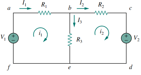
Refer to Figure 3.4, where mesh currents \(i_1\) and \(i_2\) are assigned clockwise by convention, though any direction is possible. Applying KVL to each mesh, we obtain
\[ (R_1+R_3)i_1 - R_3i_2 = V_1\] \[ -R_3i_1 + (R2+R_3)i_2 = -V_2\]
Now we can solve the simultaneous equations using the techniques of our choice.
Similar to nodal analysis with voltage sources, two methods to handle current sources in mesh analysis: 1) When a current source exists only in one mesh, the mesh current is simply set to the current value of the current source, 2) When a current source exists between two meshes, create a supermesh such that KVL can be applied to it.
3.4.3 Superposition Principle
The linearity principle states that the output of a linear circuit with multiple inputs is a linear combination of scaled inputs:
\[ y = \sum^n_{i=1} f(K_i x_i) = \sum^n_{i=1} K_i f(x_i) = \sum^n_{i=1} y_i\]
where \(x_i\) are the inputs of current or voltage and \(K_i\) are the scalar constants that are circuit-dependent.
The output is a linear combination where each input’s contribution is independent. Thus, the total output is the sum of each source’s individual response, allowing us to determine the output of a multiple input linear circuit.
- “Turn Off” all independent sources save for one, then determine the circuit’s output as a result of the influence of that single source.
- Continue the procedure in step 1 for each independent source, ensuring all other sources are turned off, and determine the output resulting from that specific source.
- The combined output from all independent sources activated simultaneously is the algebraic sum of the outputs produced by each source independently.
Switching off an independent source implies setting its value to zero, denoted as \(v_s=0\) or \(i_s=0\). In this case, a voltage source is substituted by a short circuit, and a current source by an open circuit. Does this substitution alter the circuit? The answer is no. As zero is a legitimate value for each independent source, the resulting circuit remains valid.
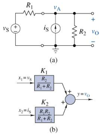
We demonstrate the superposition principle by examining the two-input circuit in Figure 3.5 (a) through node-voltage analysis. By employing KCL at node A and rearranging the terms, we obtain the equation
\[ v_o = \left[{\frac{R_2}{R_1+R_2}}\right]v_S + \left[{\frac{R_1R_2}{R_1+R_2}}\right]i_S\]
The outcome indicates that the result is a linear combination of the two inputs. A typical block diagram is depicted in Figure 3.5 (b).
3.4.4 Thevenin and Norton Equivalent Circuits
The Thevenin and Norton equivalent circuit theorems stand as foundational elements in circuit theory, often taken for granted. These theorems simplify circuit analysis significantly, and without them, circuit analysis would be difficult.
THE THEOREMS
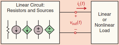
Consider a circuit with linear elements, such as resistors, dependent, and independent voltage and current sources as shown in Figure 3.6. Capacitors and inductors are excluded for simplicity, but the theorem applies to them as well. We focus on linear time-invariant circuits, although the theorems are valid for time-varying circuits as well Thomas, Rosa, and Toussaint (2016). This circuit is connected to a linear or non-linear load circuit.
Thevenin’s theorem simply states that the entire circuit can be replaced with an independent voltage source and a series resistor, which is indistinguishable from its original circuit in terms of their i-v characteristics.
Similarly, Norton’s theorem states that the entire circuit can be replaced with a single independent current source in parallel with a resistor which, again, is indistinguishable from its original circuit in terms of their i-v characteristics.
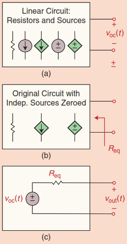
To determine the Thévenin voltage source, open the load connection and measure the open-circuit voltage \(v_{oc} (t)\) at the output port as in Figure 3.7 (a). For Thévenin resistance, disconnect the load, set all independent sources to zero, and find the equivalent resistance of the remaining circuit, which consists of resistors and dependent sources, and reduce it to a single resistor. The Thévenin equivalent circuit is shown in Figure 3.7 (c).
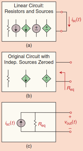
To determine the Norton current source, short the output port as in Figure 3.8 (a) and measure the short circuit current \(i_{sc} (t)\). The Norton resistance, parallel to this current source, is found exactly like the Thévenin resistance, as shown in Figure 3.8 (b). The Norton equivalent circuit is depicted in Figure 3.8 (c).
To find the equivalent resistance, zero all independent sources: short voltage sources and open current sources. But if the circuits are inaccessible, like in a black box, can we still find it? Yes, the equivalent resistance equals \(v_{oc} (t)/i_{sc} (t)\). We can easily calculate it by measuring \(v_{oc} (t)\) and \(i_{sc} (t)\) without seeing inside.
The big question is why these theorems are valid. How do you prove them? See Sheikholeslami (2018) for an intuitive proof.
Let us find the Thevenin and Norton’s equivalent of the circuit shown in Figure 3.5.
The open-circuit Thevenin voltage has already been calculated in the example to be
\[ v_{oc} = \left[{\frac{R_2}{R_1+R_2}}\right]v_S + \left[{\frac{R_1R_2}{R_1+R_2}}\right]i_S\],
and the Thevenin, Norton as well, resistance can be calculated by shorting independent voltage source and opening independent current sources, resulting in
\[ R_{eq} = R_1 || R_2 = \frac{R_1 R_2}{R_1 + R_2}\]
The Norton short-circuit current can be shown to be
\[i_{sc} = \frac{v_S}{R_1} + i_S\]
3.4.5 Max Power Transfer and Interfacing Circuits
In circuits where efficiency of power delivery is crucial, interfacing circuits have to be properly designed to ensure maximum power is delivered to the load. For example, an audio amplifier that delivers power to a speaker is typically between \(4-8 \Omega\). Or a power amplifier on a mobile phone that delivers power to the antenna which is typically \(50 \Omega\).
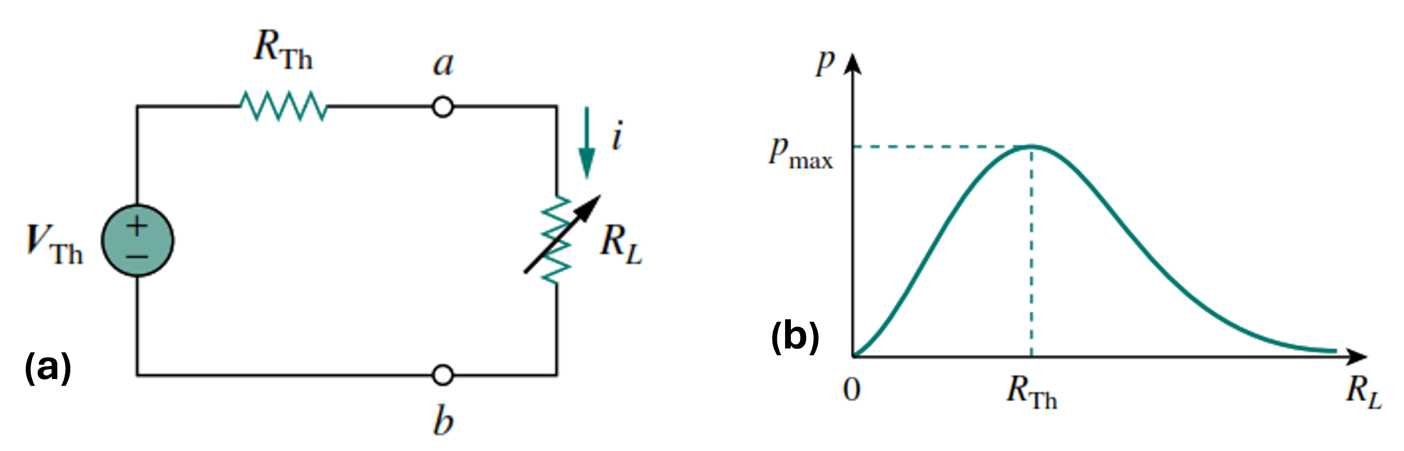
We now address the problem of delivering maximum power to a load by a circuit. This is best done by representing the circuit with it’s Thevenin (or Norton) equivalent circuit connected to the load as shown in Figure 3.9 (a) .
The Thevenin equivalent is useful for finding the maximum power a linear circuit can deliver to a load. We assume that we can adjust the load resistance \(R_L\). The power delivered to the load is
\[p = i^2R_L = \left({\frac{V_{Th}}{R_{Th}+R_L}}\right)^2 R_L\]
In a circuit with fixed \(V_{Th}\) and \(R_{Th}\), altering the load resistance \(R_L\) changes the power delivered to the load as illustrated in Figure 3.9 (b). The sketch shows that power is minimal when \(R_L\) is too small or too large, but peaks at some \(R_L\) value between \(0\) and \(\infty\). It can be shown that maximum power is achieved when \(R_L\) equals \(R_{Th}\), known as the maximum power theorem.
Maximum power is transferred to the load when the load resistance equals the Thevenin resistance as seen from the load (\(R_L = R_{Th}\))
Prove the maximum power theorem by taking the derivative of power w.r.t. the load \(R_L\) and set it to zero. (\(dp/dR_L = 0\))
Power from \(V_{Th}\) varies with \(R_L\) as \(V^2_{Th}/(R_{Th}+R_L)\), ranging from \(0\) to \(V^2_{Th}/R_{Th}\) when \(R_L\) shifts from \(\infty\) to \(0\). Most of this power is transferred to the load when \(R_L > R_{TH}\); however, if \(R_L < R_{TH}\), more power is lost in \(R_{TH}\). Therefore, maximum transfer occurs when \(R_L = R_{Th}\).
Write to program which plots \(i \text{ vs } R_L\), \(p_L \text{ vs } R_L\), and \(p_s \text{ vs } R_L\) where, \(i\) is the current drawn from the source, \(p_L\) is the power delivered to the load, and \(p_s\) is the power consumed from the source.
INTERFACING CIRCUITS
In typical applications such as an audio amplifier driving a speaker \(4~\Omega\) or a power amplifier in a mobile phone driving a \(50~\Omega\) antenna, the load is fixed and the circuit designer designs the circuit so that the source impedance \(R_{Th}\) is equal to the load \(R_L\).
There are times when the circuit designer does not have the freedom to change \(R_{TH}\) (or \(R_L\)), then an interfacing circuit is necessary to facilitate maximum power transfer.
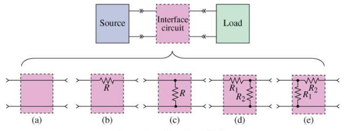
Figure 3.10 illustrates general and example resistive interface circuits. These circuits feature two terminal pairs, or ports, forming a two-port network, with an input connected to the source and an output to the load. The network ensures specific source-load interaction. There are countless interface circuit designs, but Figure 3.10 highlights five basic ones. Pass-through is simply a direct connection when design allows source or load variation. Series interfaces suit voltage-powered loads, while parallel interfaces are for current-powered loads. L-pads match fixed source and load resistances to achieve desired electrical outputs.