6 BJT Fundamentals
Bipolar Junction Transistors (BJTs) can be seen as a natural progression from the study of \(pn\) junctions. Though this text does not provide an exhaustive examination of BJTs, it will offer a basic introduction.
6.1 Principle of Operation
A Bipolar Junction Transistor (BJT) operates as a controlling element by allowing minority carriers to move through the narrow base region between the emitter and collector junctions in the active region. This region is characterized by forward-biasing the emitter-base (E-B) junction and reverse-biasing the collector-base (C-B) junction, both bias voltages exceeding by few multiples of \(\kappa T/q\). Under these conditions, the excess-carrier distribution in the base region is approximately linear as shown in Figure 6.4 . This region of operation is commonly used for linear signal amplification.
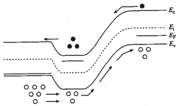
Using Figure 6.2 and Figure 6.3 as a visualizing tool, BJT valve action will be illustrated by tracking the hole diffusion current.
When forward bias is applied to the E-B junction, the emitter introduces majority carriers as minority carriers into the base. In a pnp transistor, holes travel from the p-type emitter into the n-type base, whereas in an npn transistor, electrons move from the n-type emitter into the p-type base. The forward bias elevates the surplus carrier concentrations near the emitter’s space-charge region. Typically, the emitter is more heavily doped than the base, which ensures that the E-B junction current is largely due to carriers transitioning from the emitter into the base, thereby achieving high emitter injection efficiency.
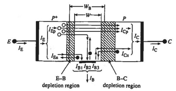
The majority of injected minority carriers diffuse through the narrow base and arrive at the reverse-biased C-B junction. The base’s thinness and a high minority carrier lifetime are essential to reduce the recombination of these carriers with the base’s majority carriers (electrons in pnp, holes in npn). Upon entering the depletion region of the reverse-biased C-B junction, the robust electric field there propels the minority carriers into the collector. Since the C-B junction is reverse-biased, there is typically no significant carrier injection from the collector to the base. Thus, the collector current mainly consists of the minority carriers injected at the emitter that have successfully crossed the base. The collector section of the reverse-biased C-B junction acts as a sink, gathering the emitted carriers post-base traversal.
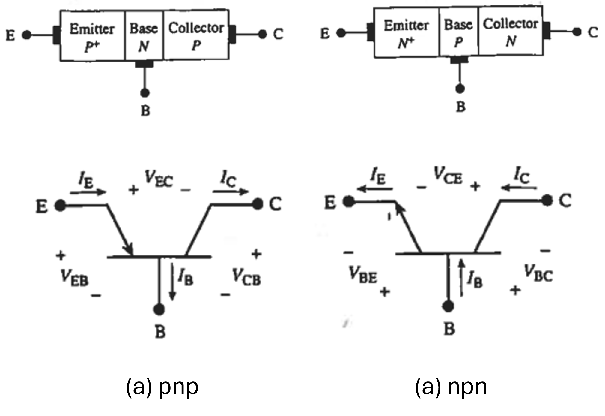
6.2 Terminal Currents
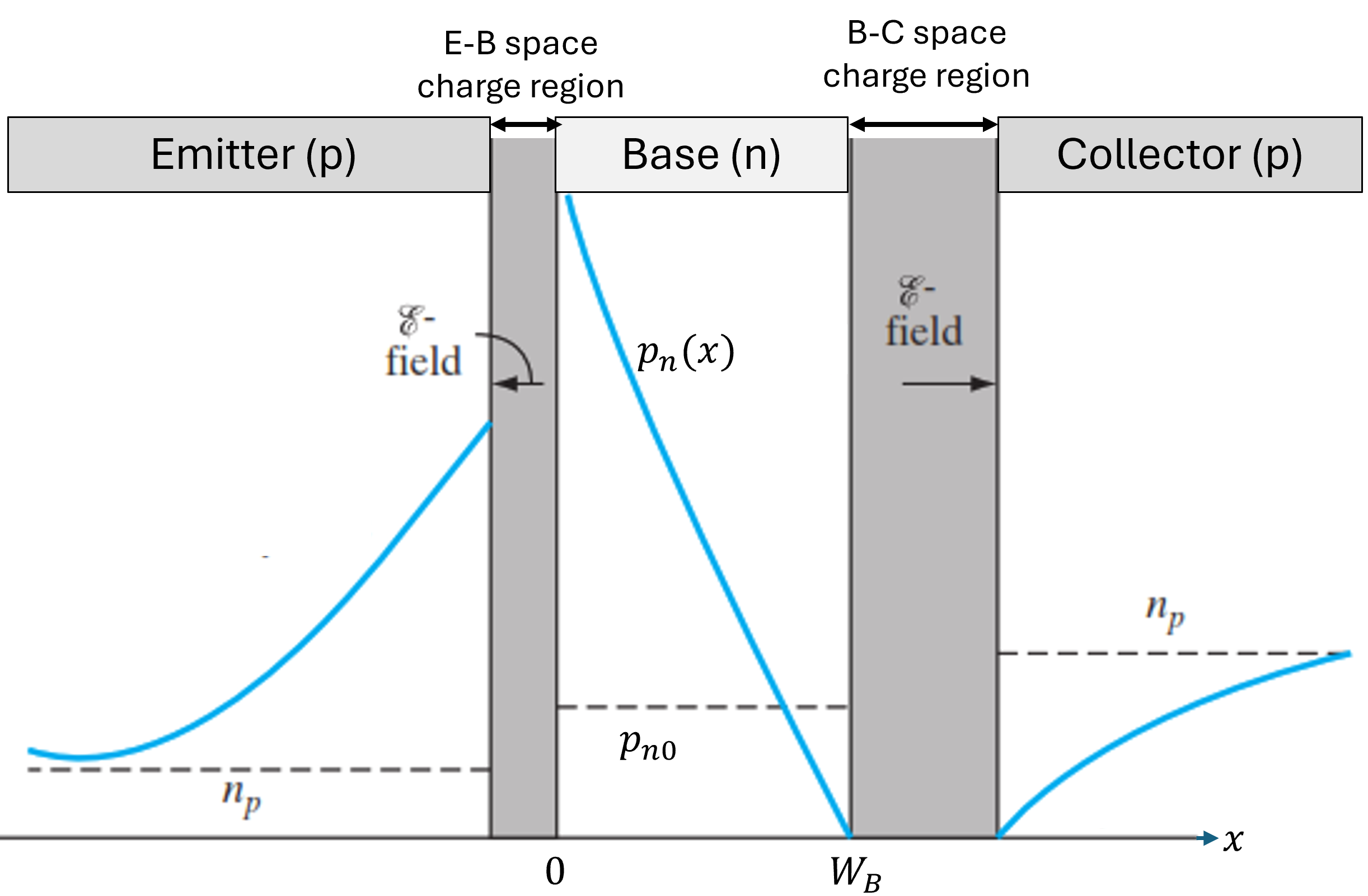
The terminal currents in the active region are linked to the excess minority carrier concentration within the base. Considering a pnp transistor, define \(p_n(x)\) as the hole concentration in the n-type base. The excess hole concentration is
\[ \Delta p_n(x) = p_n(x) - p_{n0} \]
with \(p_{n0}\) as the equilibrium hole concentration. At the space-charge layer boundaries, the excess concentrations relate to junction voltages exponentially, as in pn junction:
\[ \Delta p_E \approx p_n(0) = p_{n0} (e^{qV_{EB}/kT} - 1) \]
at the emitter junction (\(x=0\)), assuming \(p_n(0) \gg p_{n0}\).
Similarly, the excess concentration at the collector junction is:
\[ \Delta p_C = p_n(W_b) = p_{n0} (e^{qV_{CB}/kT} - 1) \approx -p_{n0} \]
at the reverse-biased collector junction (\(x=W_b\), with \(W_b\) being the base width). The excess concentration is negative due to the reverse-biased C-B junction.
In the context of a thin base with a linear excess minority carrier distribution (valid when \(W_b\) is significantly less than the diffusion length \(L_p\)), with bias assumption of few multiples of \(\kappa /Tq\), \(p_n(0) \gg p_n(W_b)\), consequently the concentration gradient is approximately \(-p_n(0)/W_b\). Therefore, the collector current \(I_C\) is linked to this gradient and can be expressed as:
\[ I_C = -qA D_p \frac{dp_n}{dx}|_{x=W_b} \]
or,
\[ I_C \approx qA D_p \frac{p_n(0)}{W_b} \]
or,
\[ I_C = qA D_p \frac{p_{n0}}{W_b} (e^{qV_{EB}/kT} - 1) \]
with \(q\) representing the elementary charge, \(A\) the cross-sectional area, and \(D_p\) the minority-carrier (hole) diffusion coefficient in the base.
In qualitative terms, increasing the forward bias \(V_{EB}\) elevates \(p_n(0)\), resulting in a sharper concentration gradient and consequently a higher collector current. In contrast, the reverse bias \(V_{CB}\) exerts a smaller impact on \(p_n(W_b)\), approximating \(-p_{n0}\), provided that it exceeds a few multiples of \(kT/q\). The emitter current \(I_E\) is composed of the hole current entering the base (\(I_{Ep}\)) and the electron current moving from the base into the emitter (\(I_{En}\)):
\[ I_E = I_{Ep} + I_{En} \]
The hole current \(I_{Ep}\) is linked to the same concentration gradient responsible for \(I_C\), while \(I_{En}\) is influenced by the majority carriers’ injection from the base to the emitter and is reduced by increasing the emitter’s doping level.
The base current \(I_B\) provides electrons for recombination with injected holes in the base and facilitates the injection of majority carriers from the base to the emitter. It is given by
\[ I_B = I_E - I_C = I_{En} + (1-B)I_{Ep} \]
where \(B\) is the base transport factor, indicating the portion of injected holes reaching the collector without recombining. A thin base with a long carrier lifetime results in \(B\) nearing one, reducing \(I_B\). All terminal currents (\(I_C\), \(I_B\), \(I_E\)) exhibit an exponential dependency on the emitter-base voltage \(V_{EB}\).
6.3 Power Amplification
Power amplification (not voltage amplification) is the desired property of a transconductance device like the BJT. The transistor amplifies because a minor variation in the base current \(I_B\) (regulated by \(V_{EB}\)) leads to a significant change in the collector current \(I_C\). This is quantified by the common-emitter current gain, \(\beta\) (also known as \(h_{FE}\)), which is the ratio of the collector current to the base current in the active region: \(\beta = \frac{I_C}{I_B}\). Given that \(B \approx 1\) (indicating negligible recombination in the base) and emitter injection efficiency
\[ \gamma = \frac{I_{Ep}}{I_{Ep} + I_{En}} \approx 1 \]
(indicating little electron injection into the emitter), we have
\[ I_C \approx I_E \]
and a small \(I_B\).
Consequently, the current transfer ratio
\[ \alpha = \frac{I_C}{I_E} = B\gamma \]
is nearly one. The common-emitter current gain \(\beta\) is described by:
\[ \beta = \frac{\alpha}{1 - \alpha} \]
As \(\alpha\) approaches 1, \((1-\alpha)\) becomes very small, making \(\beta\) large. Thus, a small base current can control a substantially larger collector current, resulting in current amplification.
Thus, Power Amplification is achieved, as the minimal power used at the input (base-emitter junction) governs a larger power output in the collector circuit. The base-to-emitter voltage directly regulates the collector current, functioning like a control valve. The excess charge in the base area directly influences the collector current and can be adjusted through the base terminal.